Thermal stress analysis of a PCB
Step-by-Step Instructions
Geometry Preparation
You can find an example geometry of a PCB board on Onshape over here.
Login to your Onshape account and then make a private copy by clicking Make a private copy option on top left.
Rename the project e.g. PCB geometry in this case (optional)
Notice that quite often, the sophisticated designs we prepare will not be suitable for simulations. A good example can be an over complex PCB which is present in the Onshape project under pcb-overcomplex tab.
To prepare the geometry for simulation, we remove unnecessary features and elements that will not influence the system much.
You can see an example of modified and prepared geometry in Onshape project under pcb-simplified tab.
Pay attention that some aspects of the geometry should be prepared before uploading it to SimScale. For example, make sure that you separate the place where electronic parts are attached to the board with extra face-cuts.
To continue with this tutorial, make sure that you have made a copy of this geometry in to your account by following steps provided above. Then you will be able to import it directly to SimScale.
Creating a new project on SimScale
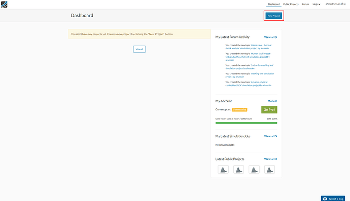
First of all you have to create a new project. For that you have to login to your account on SimScale. Once you are in your Dashboard, click New Project button
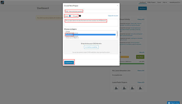
A Create New Project window will pop-up. First give your project a suitable name (this can’t be left empty) e.g. PCB - thermal stress analysis in this case. Next make sure that your project is set to Public. Add small description describing briefly about your project (this can’t be left empty). You can also define a category for your project e.g. Electronics in this case. Once done, click Create Project button.
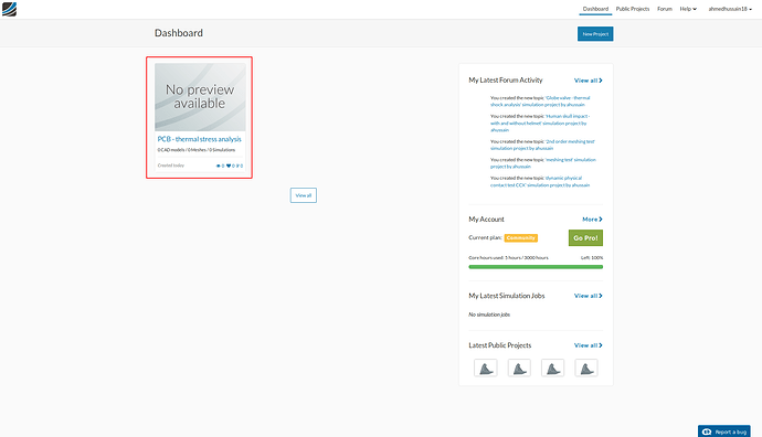
Once your new project is created you can see it in your dashboard.
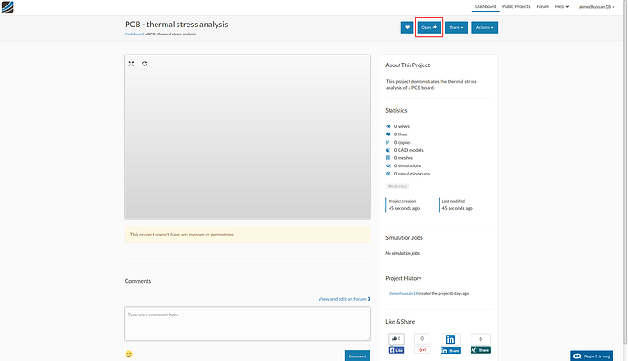
Click on the project and you will be in your project dashboard. Here you can click Open button to open your project in workspace.
Importing geometry from Onshape
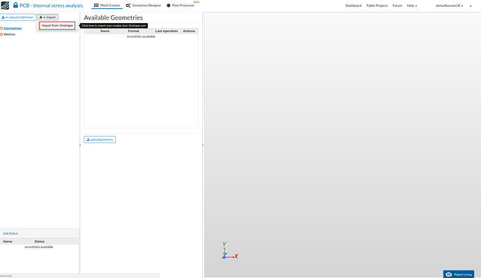
Next you can import the geometry into your SimScale workspace from Onshape. For this, click on Import and then Import from Onshape.
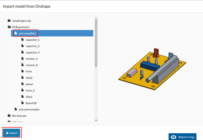
Onshape connector app window will pop-up. Login here with your Onshape credentials and allow access to SimScale (if you haven’t already). From the Onshape project list, select your project e.g. PCB geometry in this case and then select the desired geometry under this project e.g. pcb-simplified in this case. Than click Import button in order to start importing the geometry. Please note that this can take a minute or two.
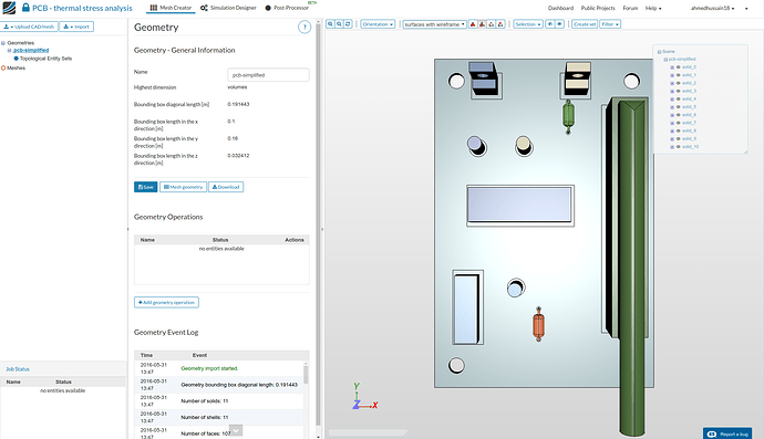
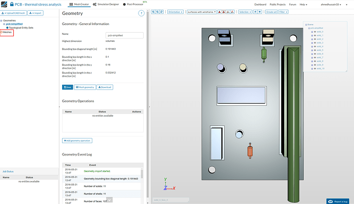
Once the geometry is imported you will see it in the viewer as shown below.
Meshing
Next you have to create a mesh in order to perform the analysis. For this, click on the Meshes item in the project tree. This will open an additional column in the middle.
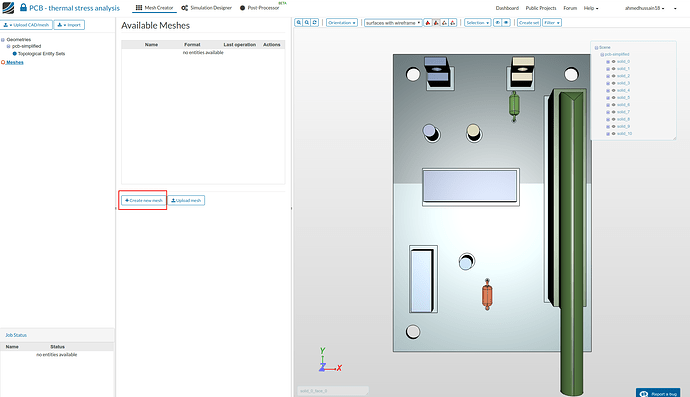
Next click the Create new mesh button to generate a new mesh.
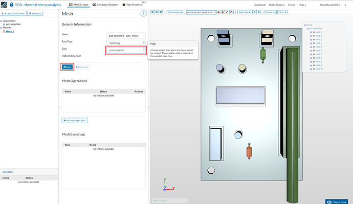
Rename your mesh (optional). Now define which geometry you want to mesh by choosing the related geometry from the Base drop-down menu. Choose pcb-simplified and click the Save button below.
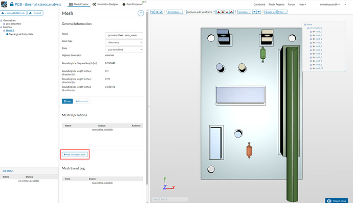
Next, click on the Add mesh operation button to create a mesh based on the geometry you selected before. This will open a new middle menu where you can specify the mesh operation you want to use to create the mesh.
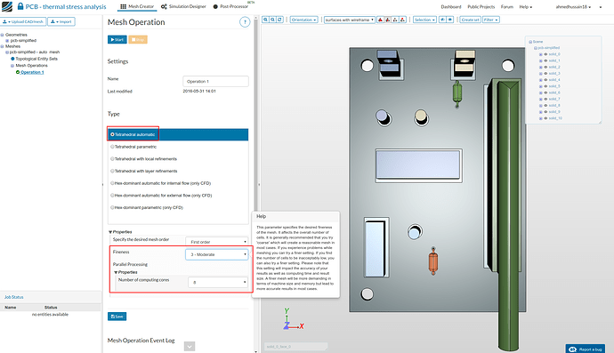
Select Tetrahedral automatic from the list and choose the following settings
-
Specify the desired mesh order: First order
-
Fineness: 3 - Moderate
-
Number of computing cores: 8
Click Save.
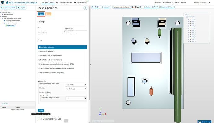
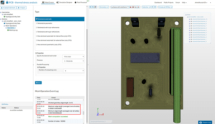
Once done, start the meshing process by clicking on the start button at top. The meshing process will take less than 10 minutes to finish.
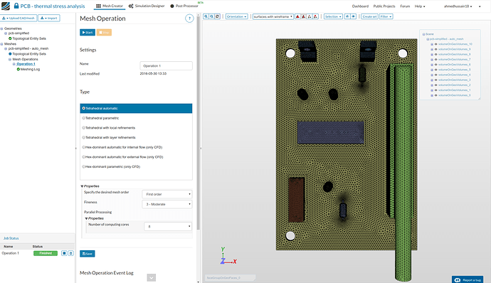
You will be notified once the mesh is computed
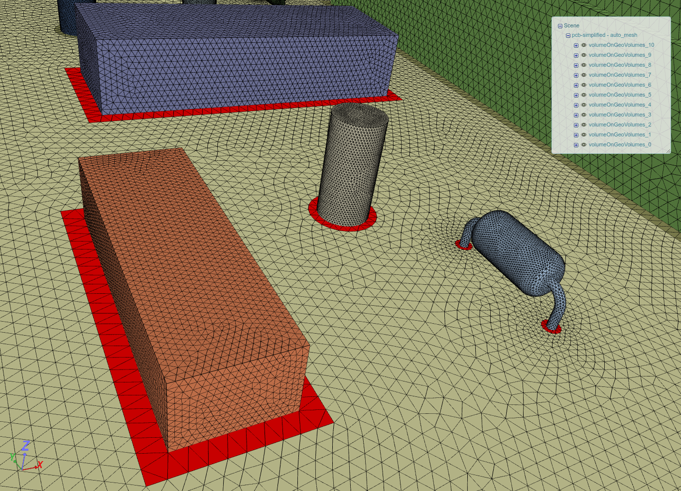
One can see that the automatic mesh didn’t capture the components nearby faces properly where the temperature change needs to be captured properly (highlighted red in figure below). Furthermore, it has also refined some parts more than usual e.g. see capacitor and resistors.
In order to produce a desired mesh, we can proceed to a manual meshing technique. To get a good idea of the manual mesh maximum and minimum edge length size, one can see the Maximum edge length (averaged over all solids) and Minimum edge length (averaged over all solids) under the Mesh Operation Event Log respectively of the auto created mesh.
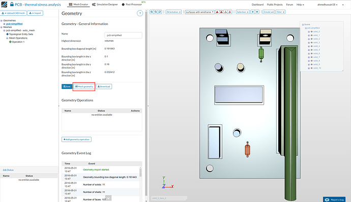
Next, go back to pcb-simplified geometry by clicking on it and then click Mesh geometry.
Doing this will automatically pick this geometry and proceed directly to mesh operation. Rename the mesh (optional).
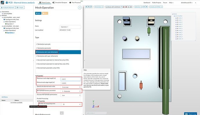
Select Tetrahedral with local refinements from the list and choose the following settings
- Set Maximum mesh edge length [m] to 0.001
- Set Minimal mesh edge length [m] to 0.0005
- Fineness: 3 - Moderate
- Number of computing cores: 32
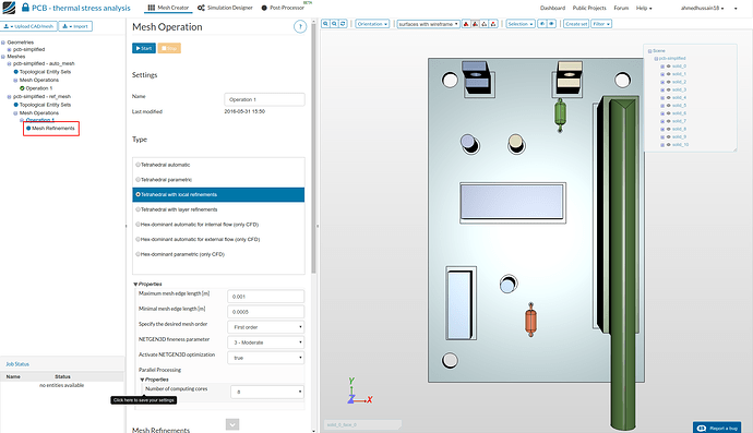
Now, scroll down to the very end and click on Save.
After saving you will see the Mesh Refinements option in the left tree.
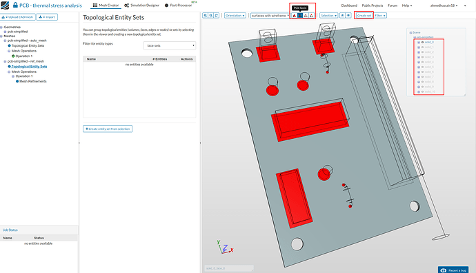
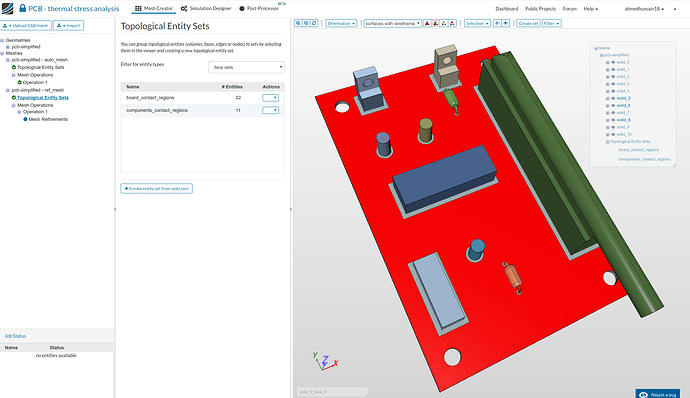
Before creating mesh refinements, let’s create the Topological Entity Sets of the regions that needs to be refined. Switch to the Topological Entity Sets from the left tree.
Topological Entity Set 1:
-
Hide all the solids except PCB by clicking the eye icon next to solids under scene tree in the viewer.
-
Make sure you are in Pick faces selection mode. If not, please switch to it above the viewer.
-
Select all the faces highlighted red in figure below.
-
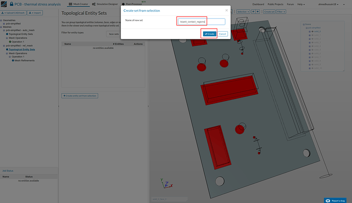
Click Create Set on top.
-
A Create set from selection window will pop-up. Give a suitable name to your set and click Create
-
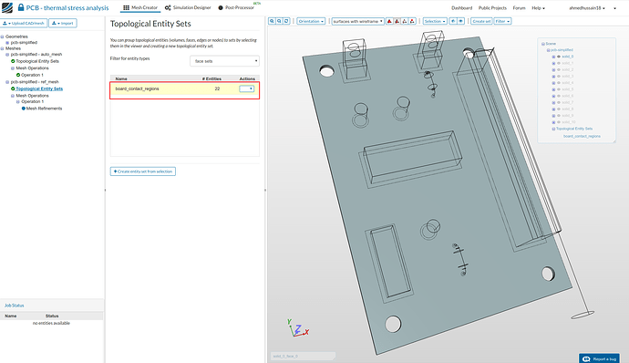
The created set will be displayed under Topological Entity Sets middle panel and should consist of 22 entities.
Before creating second topological entity set, switch back to full visible geometry by clicking Show all button above.
Topological Entity Set 2:
-
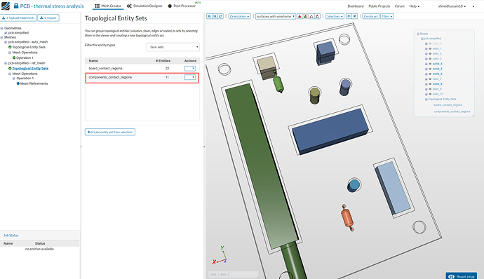
Follow the same steps as above but this time hide only PCB board and select the faces as shown below.
-
The created set will be displayed under Topological Entity Sets middle panel and should consist of 11 entities.
Before creating third topological entity set, switch back to full visible geometry by clicking Show all button above.
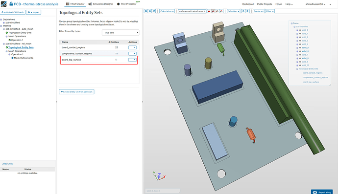
Topological Entity Set 3:
-
Follow again same steps as above and select the faces as shown below.
-
The created set will be displayed under Topological Entity Sets middle panel and should consist of 11 entities.
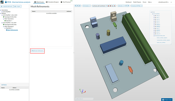
All the required topological entity sets are created. Now switch back to Mesh Refinements on left tree and click on Add mesh refinement
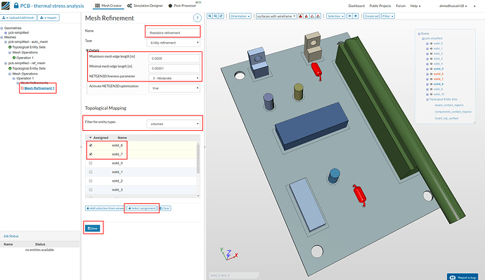
Resistors refinement:
In order to refine resistors
- Click the created Mesh Refinement 1
- Rename the mesh refinement (optional)
- Change Maximum mesh edge length [m] to 0.0005
- Change Minimal mesh edge length [m] to 0.00001
- Fineness: 3 - Moderate
- Make sure Filter for entity types is set to volumes
- Select solid_6 and solid_7 from the list
- Click Select assignment to highlight the selected volumes.
- Click Save
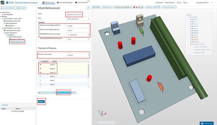
Capacitors refinement:
In order to refine capacitors
- Follow exactly the above steps and click the created Mesh Refinement 2
- This time change Maximum mesh edge length [m] to 0.0006
- Change Minimal mesh edge length [m] to 0.0001
- Select solid_8, solid_9 and solid_10 from the list
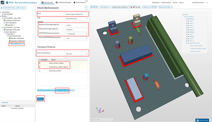
Contact regions refinement:
In order to refine contact regions
- Follow exactly the above steps and click the created Mesh Refinement 3
- Change Maximum mesh edge length [m] to 0.0001
- Change Minimal mesh edge length [m] to 0.000005
- Make sure Filter for entity types is set to face sets
- Select components_contact_regions and board_contact_regions from the list
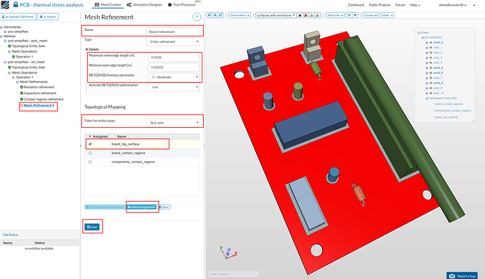
Board refinement:
In order to refine board
- Follow exactly the above steps and click the created Mesh Refinement 4
- Change Maximum mesh edge length [m] to 0.0006
- Change Minimal mesh edge length [m] to 0.00025
- Make sure Filter for entity types is set to face sets
- Select board_top_surface from the list
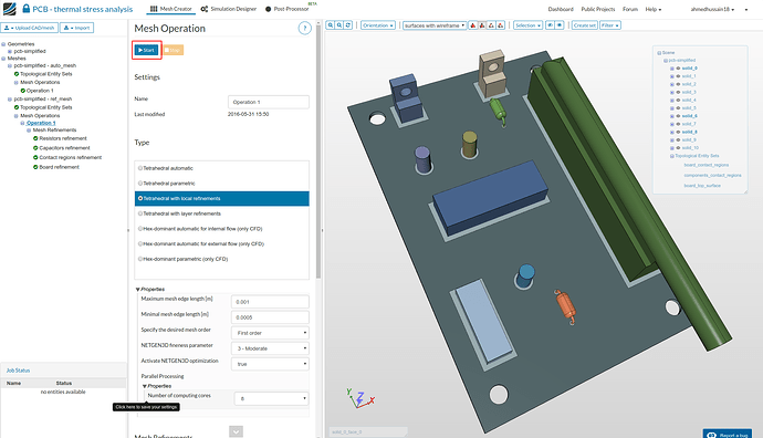
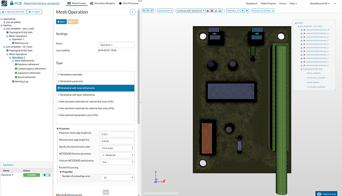
All the required refinements are done. Switch back to Operation 1 and click Start to start the meshing operation. The meshing operation may take several minutes.
You will be notified once the mesh is computed
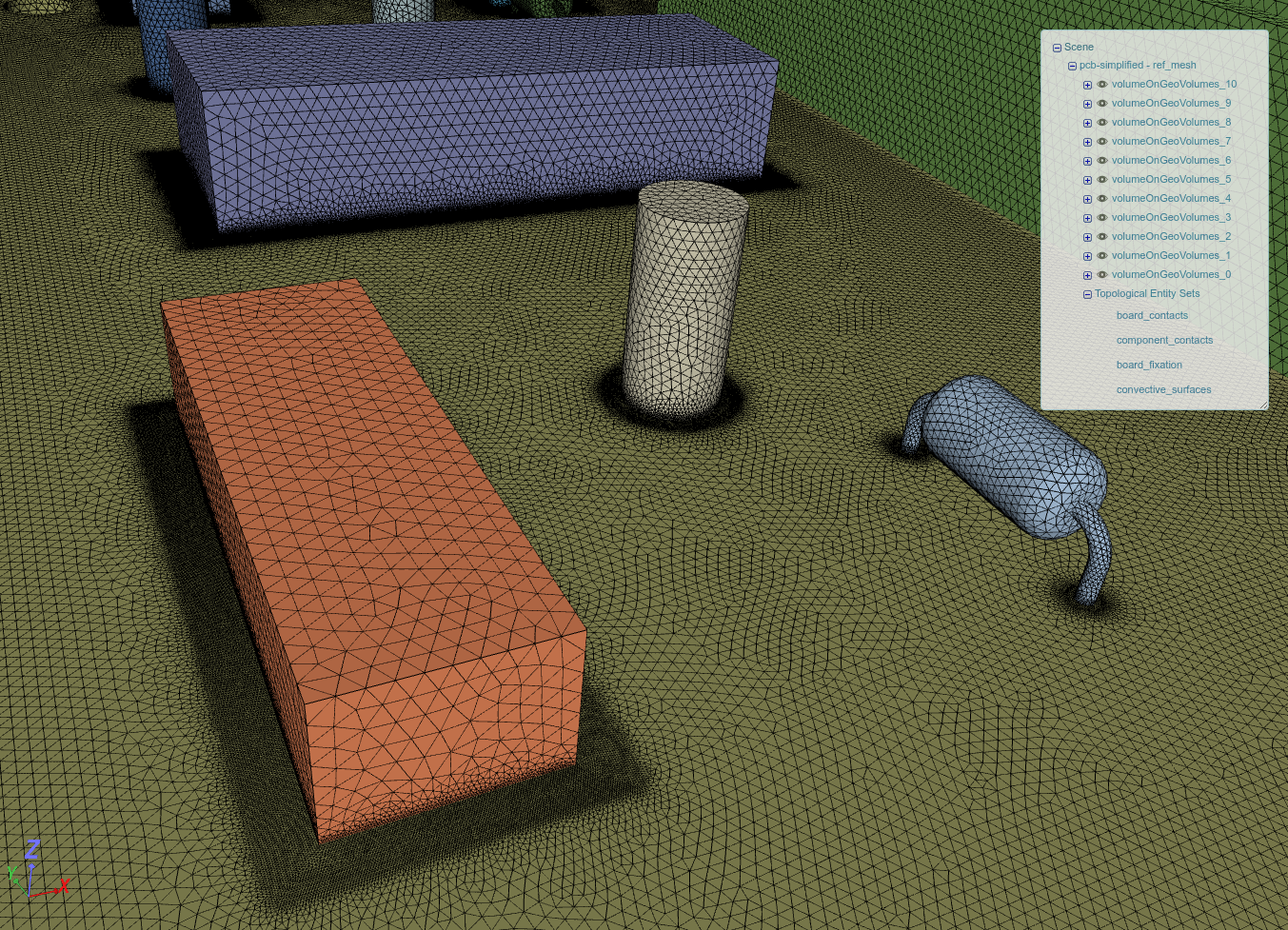
Notice now the well refined regions near the components
Simulation Setup
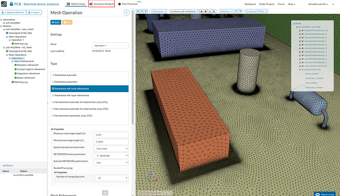
Please switch to the Simulation Designer by clicking the related button in the main ribbon bar
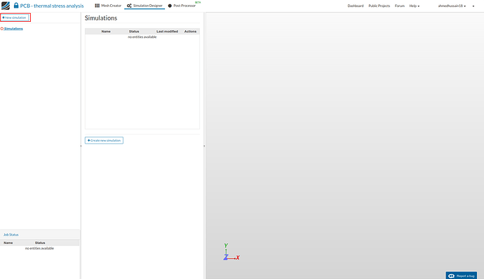
Click on the New simulation button to create a simulation run. A Create new simulation window will pop-up. Give a name to your simulation (optional) and click Create in order to create a simulation.
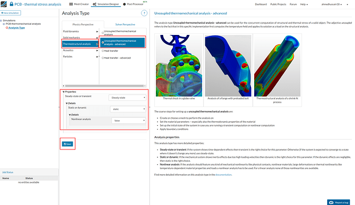
In Analysis Type, select Thermostructural analysis and then Uncoupled thermomechanical analysis - advanced. Keep the default Properties and click Save
The simulation tree on the left will be created. Entities in this tree with hollow red circle means that an operation needs to be completed, whereas filled green circle with a tick means that these entities are already taken care off and can be ignored.
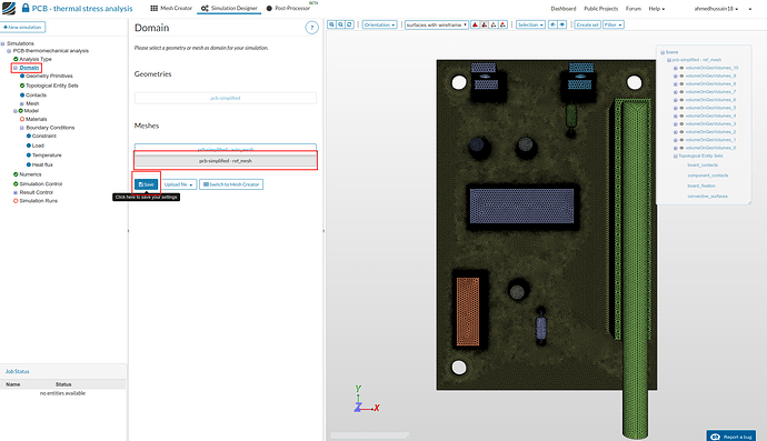
In order to perform analysis on a specific domain, we have to assign that domain to the simulation. Click Domain in left tree and select pcb-simplified-ref_mesh and click Save. This will load the assigned mesh in the viewer.
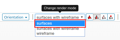
Switch the render mode to Surfaces from viewer top in order to interact with the domain more smoothly afterwards.
Since we are simulating an assembly of multiple parts it is necessary to define the interactions between them. We will therefore define this using Contacts on the left tree. Without the contacts, the solver does not knows which parts are connected to each other.
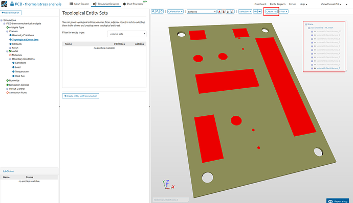
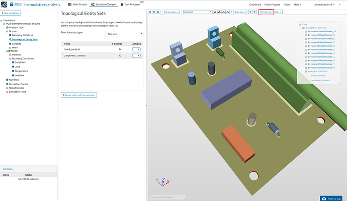
Before creating the contacts and other boundary conditions, we can create entity sets which needs to be assigned to them afterwards. The procedure for creating these Topological Entity Sets is same as we have created in meshing. In order to start creating entity sets, switch to Topological Entity Sets on the left tree.
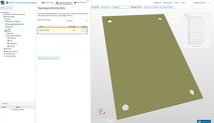
Entity set: Board contacts
- Hide the volumes except the board from the scene tree of viewer.
- Select the highlighted faces.
- Click Create set and give a suitable name and then click Create.
- The created set should contain 24 entities.
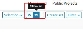
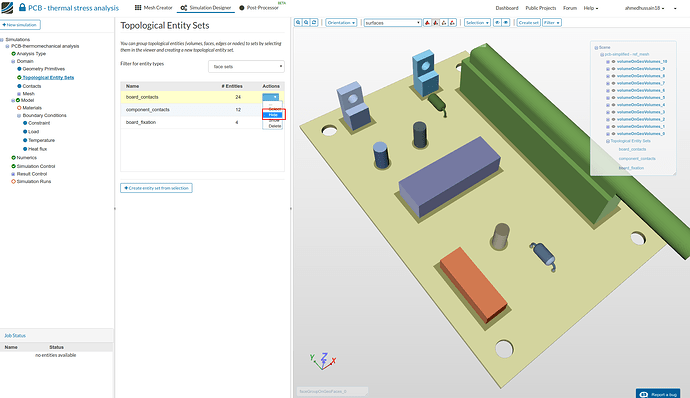
Before creating second topological entity set, switch back to full visible geometry by clicking Show all button above.
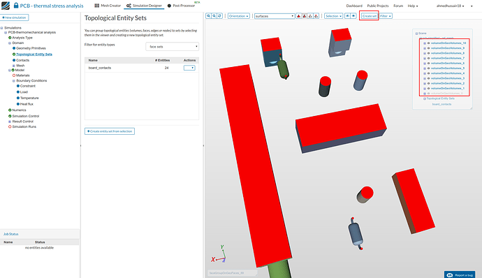
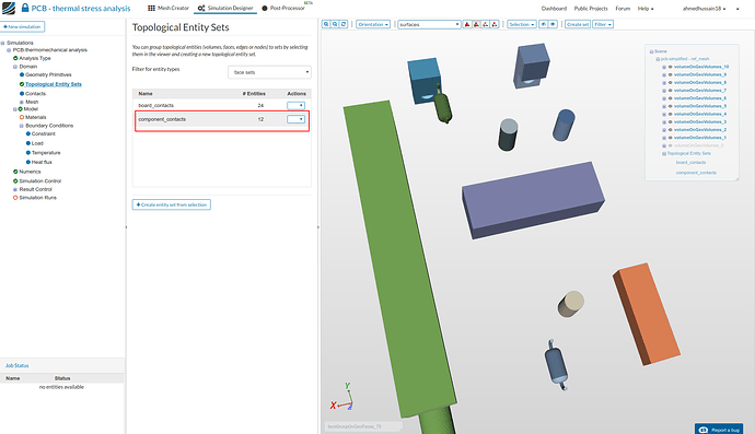
Entity set: Component contacts
- Follow same procedure as above and hide the only the board from the scene tree of viewer.
- Select the highlighted faces on the base of all the components.
- The created set should contain 12 entities.
Before creating third topological entity set, switch back to full visible geometry by clicking Show all button above.
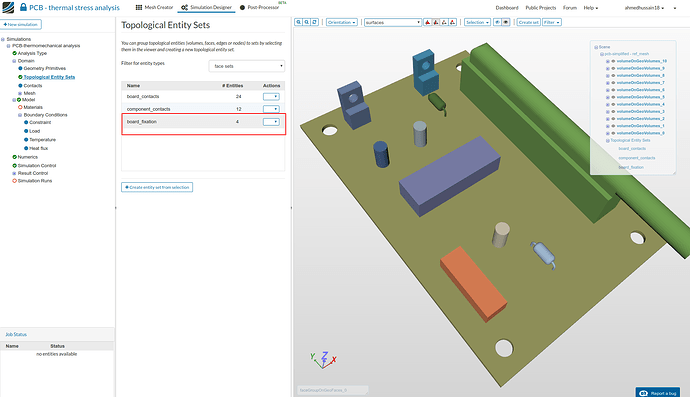
Entity set: Board fixation
- Follow same procedure as above and hide the only the board from the scene tree of viewer.
- Select the highlighted faces.
- The created set should contain 4 entities.
Before creating fourth topological entity set, switch back to full visible geometry by clicking Show all button above.
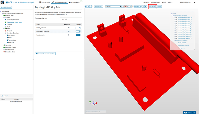
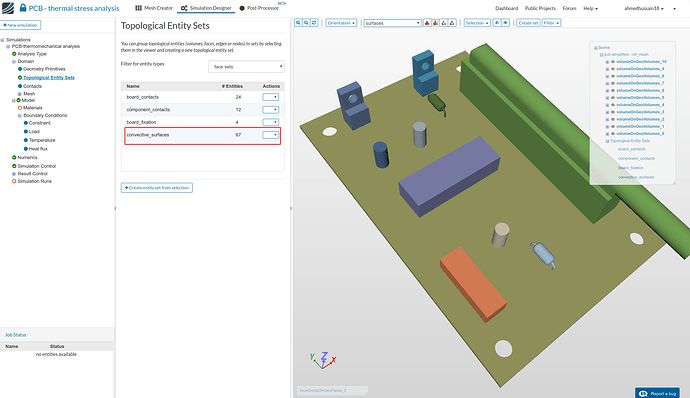
Entity set: Convective surfaces
-
Hide all the created entities one by one.
-
Click Select all from selection drop down panel above the viewer.
-
Now create the set by following the same procedure.
-
The created set should contain 67 entities.
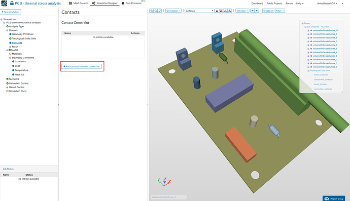
All the topological sets are now created. Next please click on the Contacts sub-item in them project tree. This will open a new middle column windows where you can manage existing and create new contacts. Click Add Contact Constraint connection.
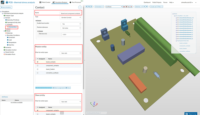
A new connection Connection 1 will be created. Give a suitable name to it (optional). Select board_contacts and component_contacts under Master entity and Slave entity respectively. Scroll all the way down and click Save.
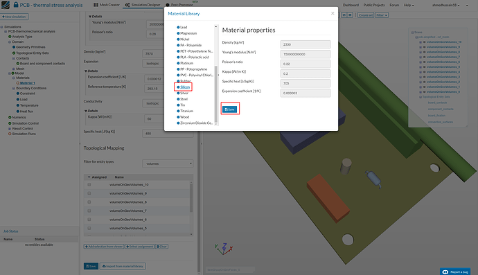
Next we have to define material for all the volumes. Click Materials in left tree and then click Add Solid material.
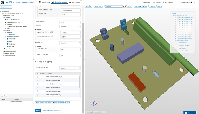
In the middle Material properties panel, scroll all the way down and click Import from material library. A material library window will pop-up. Select Silicon from it and click Save. This will load the Silicon material properties from library.
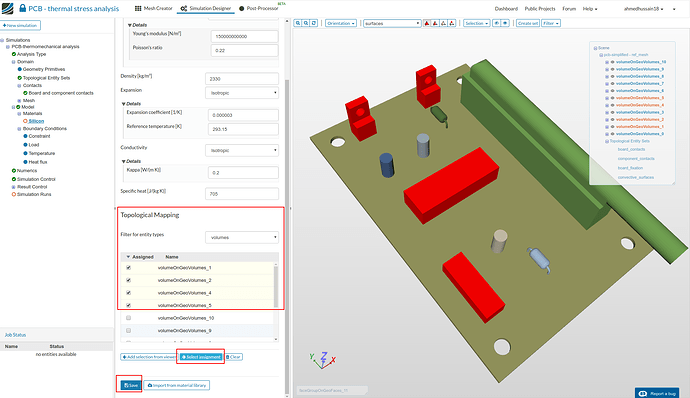
Select volumeOnGeoVolumes_1, volumeOnGeoVolumes_2, volumeOnGeoVolumes_4 and volumeOnGeoVolumes_5 and then click Select assignment. Click Save to assign the material.
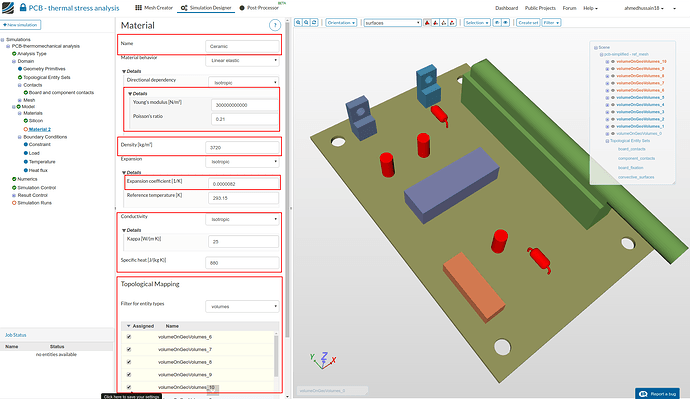
For second material, follow the same above steps. This time create a material providing your own values as shown in figure below. Change:
- Name to Ceramic.
- Young’s modulus to 300e9
- Poisson’s ratio to 0.21
- Density to 3720
- Expansion coefficient to 8.2e-6
- Kappa to 25
- Specific heat to 880
Select volumeOnGeoVolumes_6, volumeOnGeoVolumes_7, volumeOnGeoVolumes_8, volumeOnGeoVolumes_9 and volumeOnGeoVolumes_10 and scroll down to click Select assignment. Click Save to assign the material.
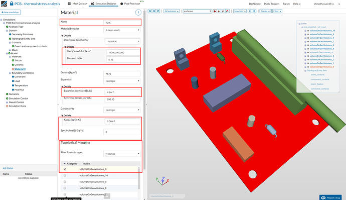
For board, follow above steps and change:
- Name to PCB.
- Young’s modulus to 113e9
- Poisson’s ratio to 0.42
- Expansion coefficient to 4.2e-7
- Kappa to 5.56e-7
- Specific heat to 0
Select volumeOnGeoVolumes_0 and scroll down to click Select assignment. Click Save to assign the material.
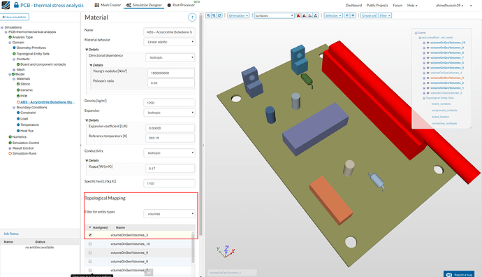
For power source, follow the same steps for importing the material from library. But this time import ABS - Acrylonitrile Butadiene Styrene from material library. Select volumeOnGeoVolumes_3 and scroll down to click Select assignment. Click Save to assign the material.
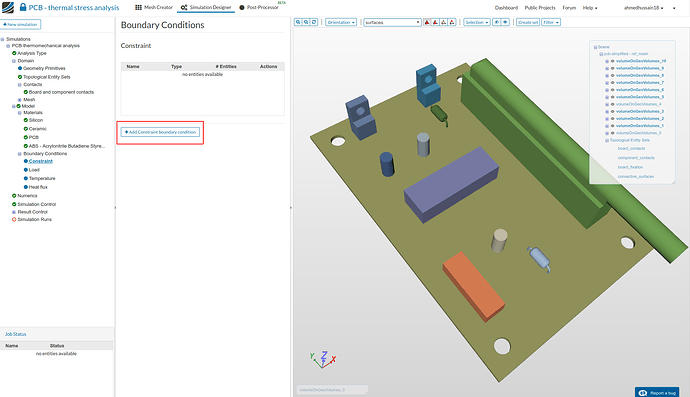
Since we are performing an Uncoupled thermomechanical analysis in which the stresses produced in the system are due to thermal change. Therefore we also have to constrain our system. To do so, select Constraint from the left tree and click Add Constraint boundary condition.
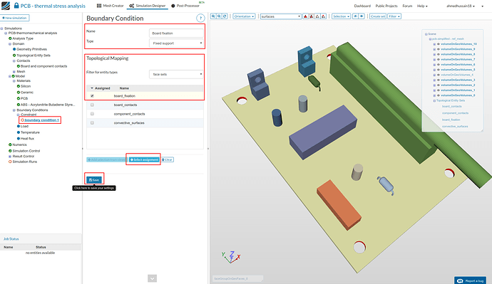
A middle Boundary Condition panel will open.
- First give a suitable name (optional).
- Next change Type to Fixed support.
- Make sure Filter for entity types is set to face sets.
- Select board_fixation and click Select assignment to see the selection in the viewer.
- Click Save to define the constraint.
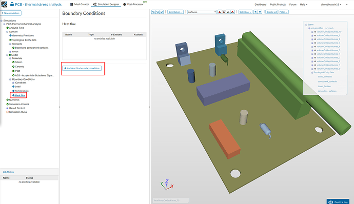
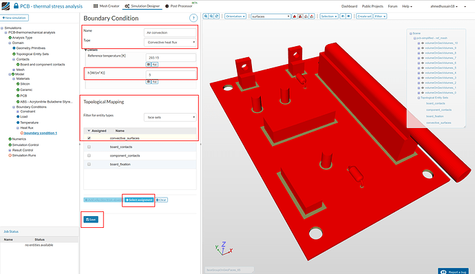
Now we proceed to define the Heat flux boundary conditions. For this click on Heat flux from left tree and then click Add Heat flux boundary condition
Heat flux: Air convection
First we will create a air convection boundary condition which will represent the convection due to air touching the outer surfaces.
- Rename the created boundary condition to Air convection (optional)
- Change Type to Convective heat flux
- Change value of convection coefficient i.e. h to 5
- Select convective_surfaces from the list
- Click Select assignment to see the selection in viewer
- Click Save to create the boundary condition
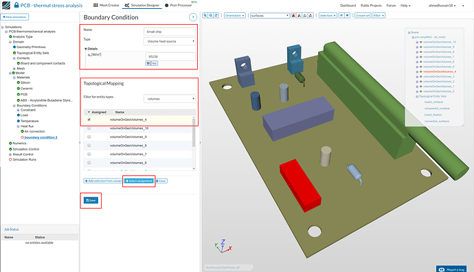
Heat flux: Small chip
By following the same procedure as above, we will now define the small chip as a heat source. The changes will be:
- Rename the created boundary condition to Small chip (optional)
- Change Type to Volume heat source
- Change value of volume heat flux i.e. qv to 95238 (0.2 W / 2.1 e-6 m3)
- Select volumeOnGeoVolumes_4 from the list
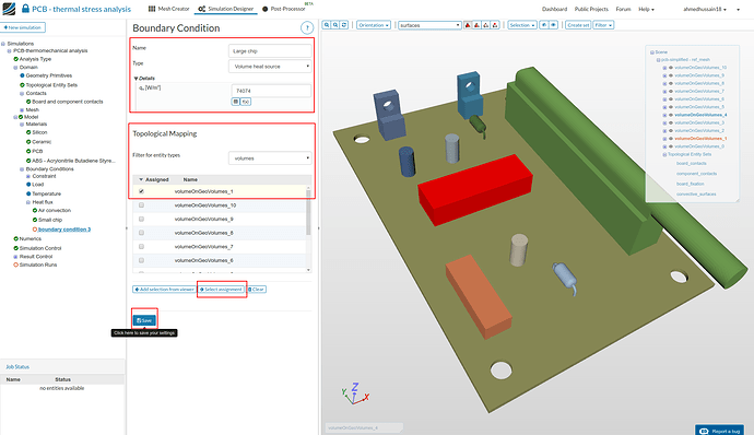
Heat flux: Large chip
Following the same procedure as in small chip case, we will now define the large chip as a heat source. The changes will be:
- Rename the created boundary condition to Large chip (optional)
- Change value of volume heat flux i.e. qv to 74074 (0.5 W / 6.75 e-6 m3)
- Select volumeOnGeoVolumes_1 from the list
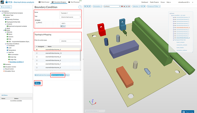
Heat flux: Transistor 1
Following the same procedure above, we will now define the first transistor as a heat source. The changes will be:
- Rename the created boundary condition to Transistor 1 (optional)
- Change value of volume heat flux i.e. qv to 53571 (0.06 W / 1.12 e-6 m3)
- Select volumeOnGeoVolumes_5 from the list
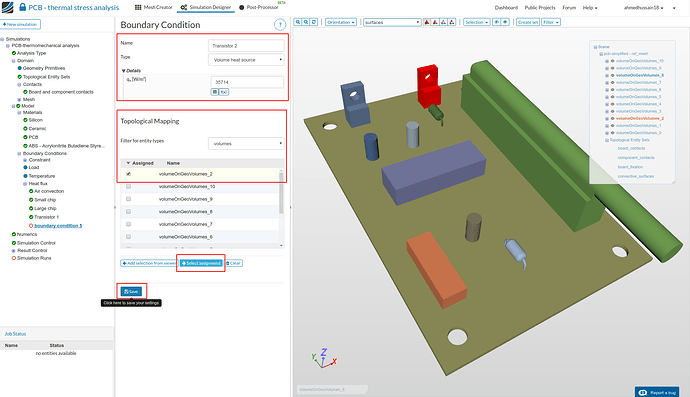
Heat flux: Transistor 2
Following the same procedure above, we will now define the second transistor as a heat source. The changes will be:
- Rename the created boundary condition to Transistor 2 (optional)
- Change value of volume heat flux i.e. qv to 35714 (0.04 W / 1.12 e-6 m3)
- Select volumeOnGeoVolumes_2 from the list
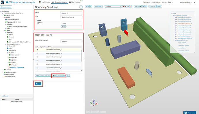
Heat flux: Resistor 1
Following the same procedure above, we will now define the first resistor as a heat source. The changes will be:
- Rename the created boundary condition to Resistor 1 (optional)
- Change value of volume heat flux i.e. qv to 73298 (0.014 W / 1.91 e-7 m3)
- Select volumeOnGeoVolumes_7 from the list
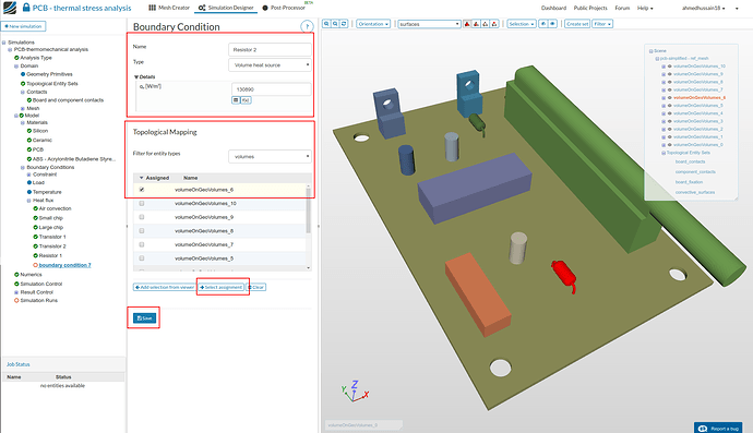
Heat flux: Resistor 2
Following the same procedure above, we will now define the second resistor as a heat source. The changes will be:
- Rename the created boundary condition to Resistor 2 (optional)
- Change value of volume heat flux i.e. qv to 130890 (0.005 W / 1.91 e-7 m3)
- Select volumeOnGeoVolumes_6 from the list
Heat flux: Capacitors
Following the same procedure above, we will now define the capacitors as a heat source. The changes will be:
- Rename the created boundary condition to Capacitors (optional)
- Change value of volume heat flux i.e. qv to 58944 (0.02 W / 3.39 e-7 m3)
- Select volumeOnGeoVolumes_8, volumeOnGeoVolumes_9 and volumeOnGeoVolumes_10 from the list
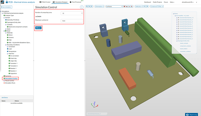
All the heat sources are now defined. Next we have to finally define the number of computing cores and maximum runtime for our simulation. For this click the Simulation Control from the left tree and then change Number of computing cores and Maximum runtime [s] to 32 and 7200 respectively. Click Save to register changes.
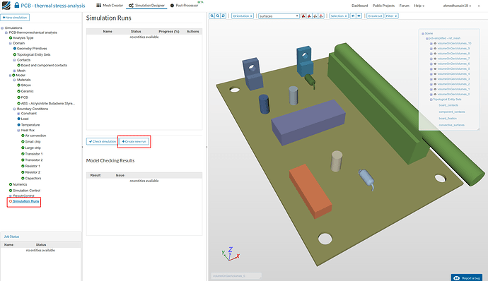
The simulation setup is now done. We have to now create a new simulation run to finally start our analysis. To do this:
- Click Simulation Run from the left tree
- Click Create new run from middle panel
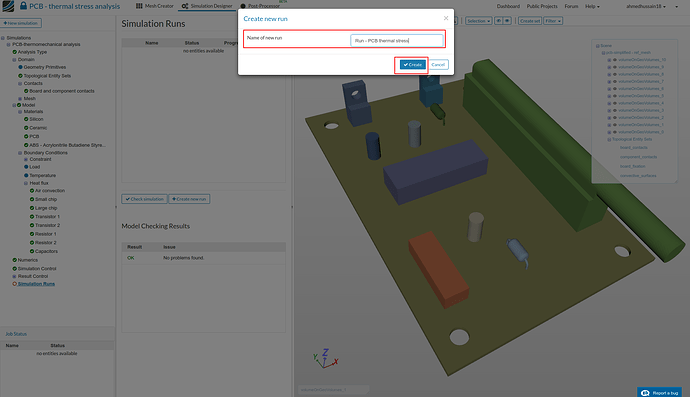
- A Create new run window will pop-up. Rename the run (optional) and then click Create
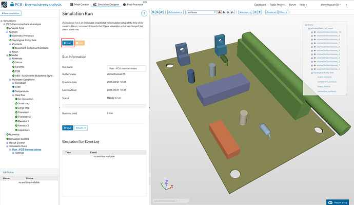
- A simulation run with your described name will be created. Finally click Start to start the simulation run
Post Processing
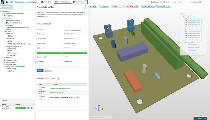
Once your simulation is finished, please click on the Post-Processor button in the main ribbon bar.
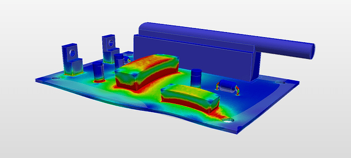
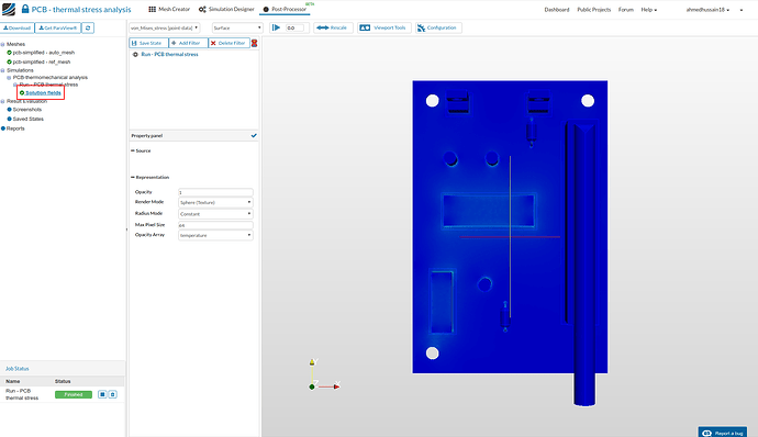
Next we will take a look at the 3D result. Click on the Solution fields item in the project tree. After a minute or two, the geometry will be loaded to the post processing viewer. The default solution field value is vonMises stress.
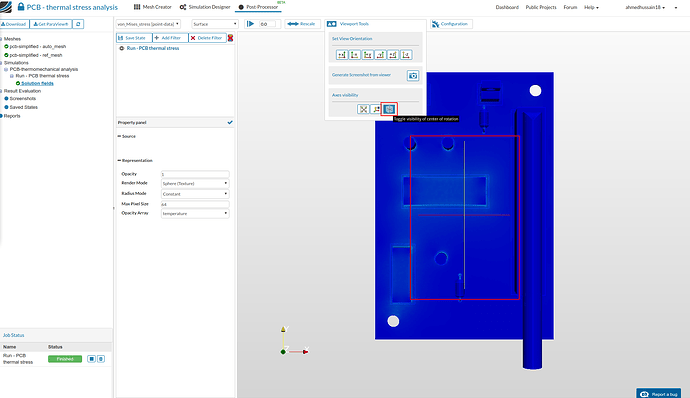
First let’s create a first screenshot which will become a thumbnail of the project. For this, first go to Viewport Tools and turn off the Toggle visibility of center of rotation option. This will turn of the center of rotation axis.
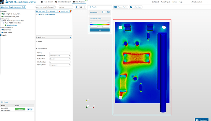
Next, rescale the value via Rescale option from viewer top from 0 to 1e7 and click OK. This will rescale the vonMises stress to this range.
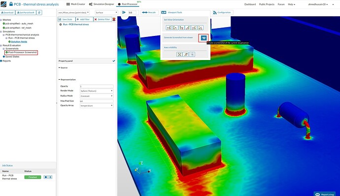
Now align the geometry to the angle of your choice and click the camera button under Viewport Tools. This will create your first post processing screenshot with a default name of Post-Processor Screenshot. You can rename it to your liking.
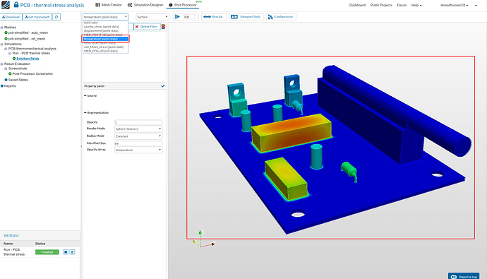
Next you can switch your results from vonMises stress to temperature. To do this, click on the Array Name over the middle panel and then click temperature [point-data]. This will show the results in the viewer based on temperature solution field.
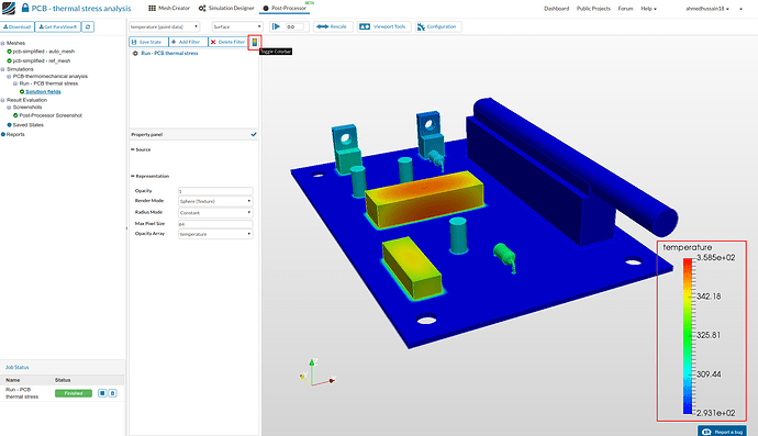
In order to see the color bar, click on the Toggle Colorbar button next to Delete filter in middle panel. This will turn on the color bar for temperature.
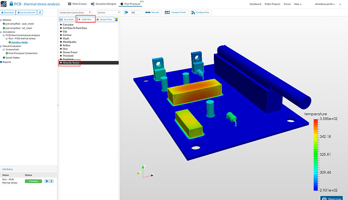
Finally to see the deformed PCB due to heated components, click on Add Filter in middle top of the mid panel and select WarpByVector
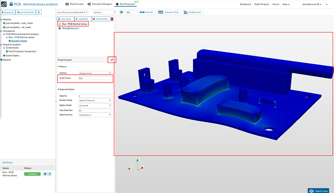
A WarpByVector1 filter will be created. Next:
- Turn off the Run - PCB thermal stress filter by clicking the eye button on it’s left
- Click WarpByVector1 filter and change the Scale Factor value to 500. This will scale the deformation to 500 times
- Click blue tick
- The deformed shape will be then visible in the viewer.
